2014-05-02 - SPI@ATmega64(A)
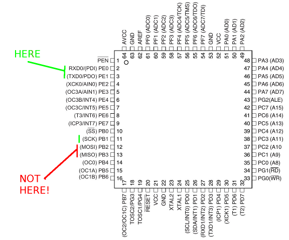
while doing an AVR-based project with friends, we decided to switch from ATmega169 to ATmega64A, which has 4x more program memory and is easier accessible on retail market. after soldering µC on our prototype board we were unable to flash it. 4 ppl checked the schema twice to see if SPI is connected to proper MISO, MOSI, SCK and reset pins. cable has been checked… and then one of friends found an interesting post on the net, saying that SPI from programming ATmega64(A) should be connected to PE0 and PE1, instead of PB2 and PB3, as pinout suggest:
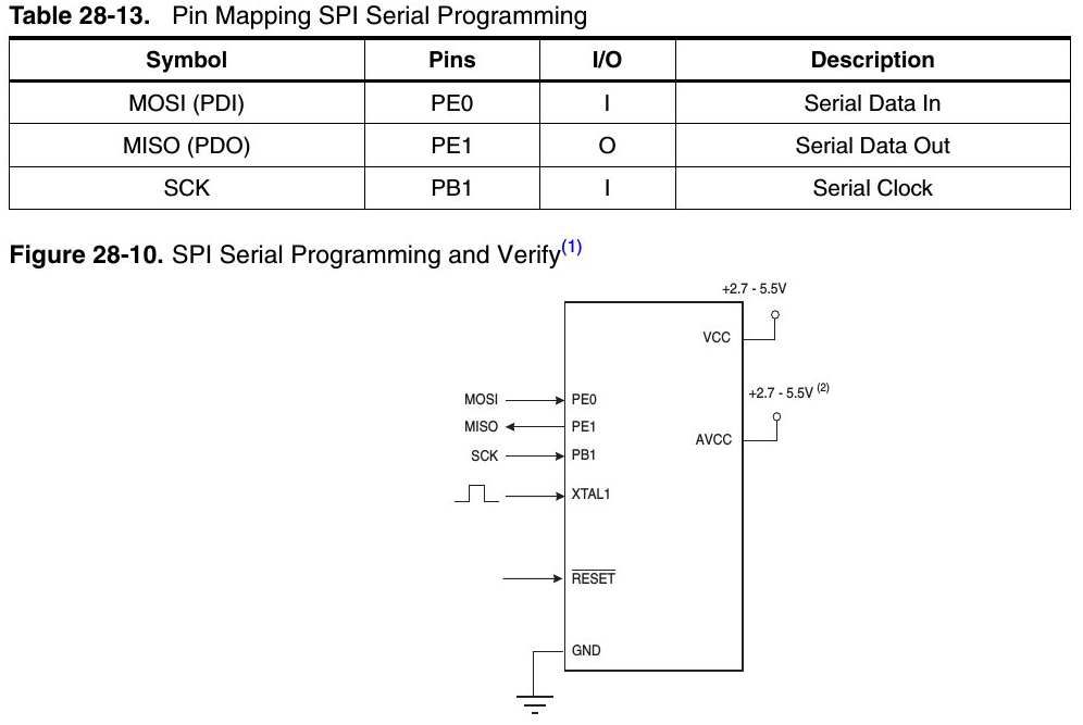
a bug this big in a datasheet? at first i though this might be a matter of a bootloader – PE0 and PE1 cab be used by USART0, after all. after having a quick look at an ATmega64A datasheet, section 28.8 resolved a mystery:
quoting:
Even though the SPI Programming interface re-uses the SPI I/O module, there is one important difference: The
MOSI/MISO pins that are mapped to PB2 and PB3 in the SPI I/O module are not used in the Programming interface.
Instead, PE0 and PE1 are used for data in SPI Programming mode as shown in Table 28-13.
so this is a feature, not a bug, after all… how obvious and how convenient! looking though forums shows that many ppl fall into this trap around the world. despite this is tricky, this is not the way it is done in other popular AVRs, like ATmega8, ATtiny13 and others, i had worked with before.
The nice thing about standards is that you have so many to choose from.
– Andrew S. Tanenbaum

